
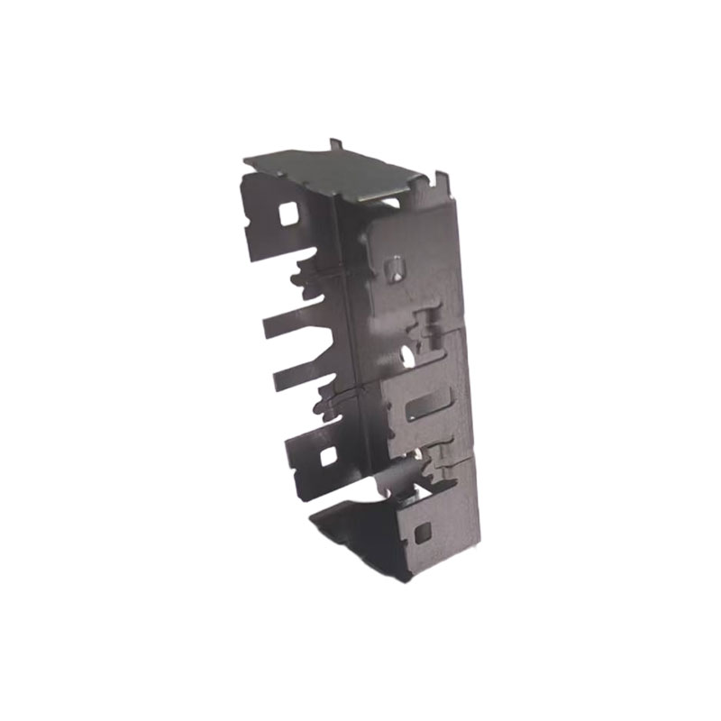
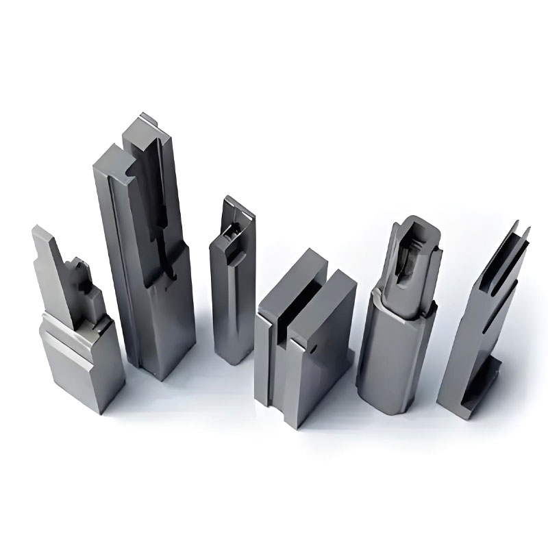
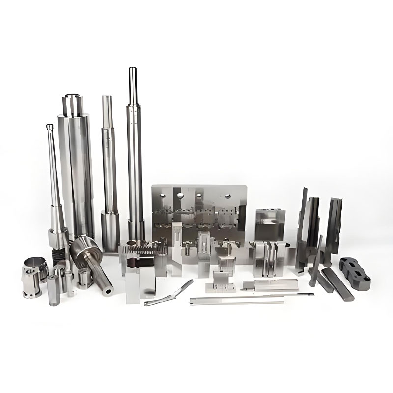
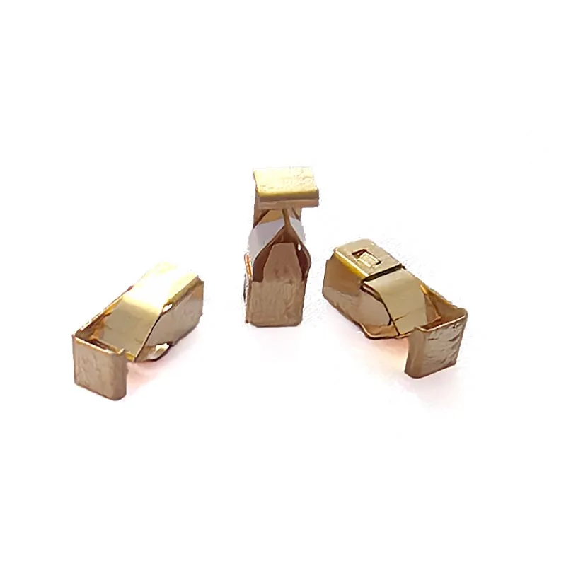
Electronic Precision Stamping Parts are essential for producing compact, conductive, and highly accurate components used in connectors, sensors, automotive electronics, and communication devices. Qiren combines precision stamping with EDM technology to manufacture complex metal components with dimensional tolerances down to ±0.005 mm, supporting both prototype development and high-volume production.
As electronic products become smaller, thinner, and more integrated, manufacturers need metal components that can maintain tight dimensions while delivering stable conductivity, mechanical strength, and reliable assembly performance. Electronic precision stamping provides an efficient way to form terminals, contact components, shielding parts, spring elements, and other intricate metal structures at production scale. By combining EDM mold manufacturing, precision stamping, intelligent inspection, and process control, Qiren provides customized solutions for electronics, automotive electronics, medical equipment, and communication applications. Its reported ±0.005 mm dimensional tolerance capability, material adaptability, and surface-quality control make precision stamping suitable for demanding electronic component applications.
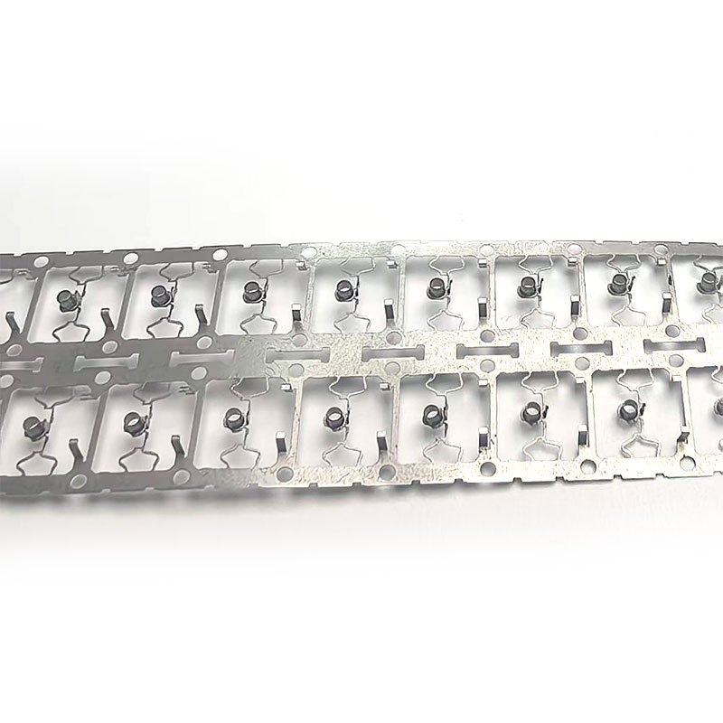
Table of Contents
- Why Are Electronic Precision Stamping Parts Important?
- What Are the Main Advantages?
- Which Materials Can Be Used?
- How Are Precision Stamping Parts Manufactured?
- Where Are They Used?
- How Should Buyers Select a Precision Stamping Supplier?
- Frequently Asked Questions
- Conclusion
Why Are Electronic Precision Stamping Parts Important?
Modern electronic products increasingly depend on miniature metal components. A connector terminal, shielding element, contact spring, battery component, or conductive support may be only a fraction of the size of a conventional mechanical component, yet it can directly influence the performance of the complete product.
This is why precision stamping is more than simply cutting and forming sheet metal. The manufacturing process must control dimensional accuracy, material deformation, burrs, surface quality, and repeatability. For electronic applications, even a small dimensional deviation can affect contact pressure, insertion force, electrical conductivity, assembly alignment, or product lifespan.
According to Qiren's product information, its stamping operation combines EDM mold processing with precision stamping and inspection technologies. The company states that its process can achieve tolerances as tight as ±0.005 mm for suitable applications, including complex-shaped parts, micro-hole components, and ultra-thin materials below 0.1 mm.
This combination makes precision stamping particularly valuable when manufacturers need repeatable components in large quantities without sacrificing dimensional consistency.
What Are the Main Advantages of Electronic Precision Stamping Parts?
1. High Dimensional Accuracy
Precision electronic components often require tightly controlled dimensions to fit miniature assemblies. Advanced die design, EDM machining, and controlled stamping parameters can reduce dimensional variation and improve part-to-part consistency.
For connector terminals and other conductive components, dimensional accuracy directly influences mating performance. Consistent geometry helps manufacturers maintain predictable insertion force, contact positioning, and assembly compatibility.
2. Complex Geometry Capability
Traditional stamping processes may face limitations when components contain deep grooves, sharp corners, stepped holes, narrow sections, or other intricate features. EDM-assisted tooling can help create more sophisticated die structures for these demanding geometries.
- Micro holes and narrow slots
- Stepped and recessed structures
- Fine contact areas
- Sharp-angle features
- Ultra-thin metal components
- Small spring and conductive structures
3. Efficient Mass Production
Once the stamping die has been developed and validated, the process can produce large quantities of consistent parts with relatively short cycle times. This makes precision stamping particularly attractive for electronics manufacturers with stable production volumes.
4. Better Surface Quality
Surface condition is critical for electrical and mechanical components. Excessive burrs, scratches, deformation, or rough surfaces can create assembly problems or negatively influence conductivity and wear resistance.
Qiren describes the use of non-contact EDM processing and mirror-finishing technology for demanding applications, with reported surface roughness below Ra0.2 μm under applicable processing conditions.
Which Materials Can Be Used?
Material selection should be based on conductivity, strength, corrosion resistance, hardness, spring characteristics, forming behavior, operating temperature, and final application requirements.
| Material Type | Typical Characteristics | Potential Applications |
|---|---|---|
| Copper Alloys | Good electrical conductivity and formability | Terminals, contacts, conductive components |
| Stainless Steel | Strength, corrosion resistance, durability | Electronic housings, springs, structural components |
| Titanium | High strength-to-weight ratio and corrosion resistance | Specialized electronic and medical components |
| High-Hardness Alloys | Wear resistance and mechanical stability | Demanding precision components and tooling-related parts |
Choosing the correct material also affects die life and production cost. Materials with high hardness or toughness may require specialized tooling and machining strategies, making engineering analysis important before mass production.
How Are Precision Stamping Parts Manufactured?
A reliable precision stamping project normally begins long before the first production run. The component drawing, material specification, tolerance requirements, surface finish, annual volume, and application environment should all be reviewed during the engineering stage.
Step 1: Product and Drawing Analysis
Engineers evaluate the geometry, tolerances, material thickness, forming direction, critical dimensions, and potential manufacturing risks. Early design analysis can help identify features that may create deformation, cracking, excessive burrs, or difficult tool maintenance.
Step 2: Precision Die Design
The stamping die determines how accurately the final component can be formed. For complex electronic parts, EDM machining can be used to create fine structures and high-precision die features.
Step 3: Material Preparation
The selected metal strip or sheet must meet the required thickness, mechanical properties, and surface condition. Material consistency is particularly important when extremely tight tolerances are involved.
Step 4: Stamping and Forming
During production, the material passes through controlled stamping operations to achieve cutting, bending, punching, forming, or progressive features. Stable process parameters help maintain repeatability throughout the production batch.
Step 5: Dimensional and Surface Inspection
Inspection verifies critical dimensions and detects potential defects. Qiren reports using three-dimensional measuring equipment, optical inspection equipment, and hardness testing as part of its quality-control process. Batch quality reports can also support production traceability and customer acceptance.
Where Are They Used?
Electronic precision stamping components are used across multiple industries because they can combine small dimensions with high repeatability and functional reliability.
Consumer Electronics
Smartphones, laptops, wearable devices, and other compact products require miniature metal components that fit accurately into restricted internal spaces. Applications can include SIM card holders, Type-C interface components, contact terminals, and FPC-related metal structures.
Automotive Electronics
The increasing use of electronic control systems and electric vehicles has expanded demand for precision conductive and mechanical components. Potential applications include battery-related components, relay springs, terminals, sensor components, and electrical connection systems.
Medical Equipment
Medical devices can require miniature components with controlled dimensions and reliable surface quality. Precision-stamped metal parts may be used in micro-instrument components, device housings, and other specialized assemblies where dimensional consistency is essential.
Communication Equipment
Communication devices and high-density electronic assemblies rely on accurate connectors and conductive components. Precision stamping can support the production of compact contact structures that require consistent geometry during repeated assembly.
How Should Buyers Select a Precision Stamping Supplier?
Selecting the right supplier is not simply a matter of comparing unit prices. For precision electronic components, tooling capability, inspection systems, material experience, engineering support, and production scalability can have a greater impact on the total project cost.
Before placing an order, buyers should evaluate the following points:
- Dimensional capability: Confirm whether the supplier can consistently meet the required tolerances.
- Tooling expertise: Review the supplier's die design, EDM, maintenance, and optimization capabilities.
- Material experience: Make sure the manufacturer understands the selected copper alloy, stainless steel, titanium, or other material.
- Inspection capability: Check whether critical dimensions can be measured using appropriate CMM, optical, or other inspection equipment.
- Production scalability: Ensure the supplier can move from prototype or trial batches to stable mass production.
- Quality documentation: Ask for inspection reports and clearly defined acceptance criteria.
- Engineering communication: A responsive technical team can reduce unnecessary tooling revisions and production delays.
Qiren states that its stamping operation supports both small-batch trial production and larger-scale manufacturing. Its production information also highlights a 3,000-square-meter facility, more than 50 employees, and an R&D team representing approximately 15% of its workforce. The company reports exports to more than 20 countries and regions.
Frequently Asked Questions
What are Electronic Precision Stamping Parts?
Electronic Precision Stamping Parts are accurately formed metal components manufactured through precision stamping processes for electronic and electromechanical applications. They can include terminals, contacts, springs, shielding components, conductive supports, and other miniature parts.
What tolerance can precision stamping achieve?
The achievable tolerance depends on material, geometry, thickness, tooling design, and production conditions. Qiren reports dimensional tolerances down to ±0.005 mm for suitable precision stamping applications. Actual tolerances should be confirmed against the specific part drawing.
Can complex electronic components be customized?
Yes. Custom precision stamping can be developed around customer drawings, 3D models, material specifications, dimensions, tolerances, surface requirements, and production volumes. EDM-assisted die manufacturing is particularly useful for intricate structures that are difficult to produce with conventional tooling.
Which industries use precision electronic stamping components?
Major application areas include consumer electronics, automotive electronics, medical equipment, communication equipment, smart-home products, and other precision electronic assemblies.
How can I request a quotation?
Providing a 2D drawing or 3D CAD file, material information, annual quantity, critical tolerances, surface-finish requirements, and expected delivery schedule can help a manufacturer evaluate the project and prepare a more accurate quotation.
Conclusion
As electronic devices continue to become smaller and more sophisticated, manufacturing accuracy is becoming increasingly important. Electronic precision stamping provides a practical combination of dimensional consistency, complex-forming capability, material flexibility, surface quality, and scalable production. With EDM-assisted tooling, controlled stamping, and systematic inspection, manufacturers can produce miniature metal components that meet demanding electronic assembly requirements.
Qiren combines precision mold engineering, EDM processing, stamping, and inspection capabilities to support customized electronic component projects from tooling development through production. If you are sourcing high-accuracy metal components for connectors, automotive electronics, medical devices, communication equipment, or other precision assemblies, contact us to discuss your drawings, materials, tolerances, production volume, and customized stamping requirements.